Semiconductors: Driving Modern Society
Semiconductors are virtually everywhere. Almost every electronic product around us contains semiconductors—from small devices like mobile phones, smartwatches, and headphones, to mid-sized appliances like computers, microwaves, rice cookers, and refrigerators, all the way to cars, metro systems, and airplanes. What makes semiconductors so incredible? And why is TSMC, a semiconductor foundry, often referred to as Taiwan’s “guardian mountain”?
Semiconductors: Components That Control Electricity (and Magnetism)
What makes semiconductors so powerful is their ability to control current and voltage. That might not sound like a big deal at first, but if we take a macro view, the operation of every electrical appliance and gadget relies on the precise control of electricity.
Beyond controlling current and voltage, semiconductors can also amplify signals. For instance, speakers work on the principle that electric current produces an electromagnetic field. By controlling the current at specific frequencies, the speaker vibrates along with the air to produce sound. Because the raw signal current is very weak, connecting it directly to a speaker would produce very faint audio, or none at all. Semiconductors can amplify this current, allowing even tiny signals to drive a speaker.
It All Starts with Sand
The primary component of sand is silicon dioxide (). Through refining, it yields crude silicon—the foundational material of semiconductors: silicon.
Next, it undergoes distillation and other chemical processes to achieve ultra-high purity, as impurities can easily introduce defects. Then comes the manufacturing of silicon wafers, the core building blocks for ICs (Integrated Circuits). Through various fabrication processes, circuit patterns are printed onto the wafer, which is then sliced, packaged, and tested to become the ICs we see today. The whole process sounds simple in theory, but turning sand into wafers isn’t something you can cook up at home on the stove. Every single step demands the full resources and cutting-edge technology of specialized companies.
When you think about packing billions of transistors into a tiny CPU and having it function flawlessly, it is nothing short of a miracle of human civilization.
Yet what amazes me most is that the ubiquitous sand found in nature forms the bedrock of modern human technology. In the end, it all traces back to nature.
What Makes Silicon So Special?
Now that we know semiconductor materials originate from sand (after extensive processing), what unique properties make the semiconductor industry so dependent on silicon? First, it is important to clarify that silicon is not the only material capable of acting as a semiconductor; silicon is used primarily because its raw material is abundant and easy to acquire.
The key lies in silicon’s atomic structure. Silicon has four valence electrons in its outermost shell. When energized, these electrons can relatively easily break free from the atom to become free electrons. Once electrons can move freely, electric current can flow.
An atom’s conductivity depends on how easily its valence electrons can become free electrons. Insulators hold onto their electrons tightly, making it nearly impossible for them to break free. Conductors, on the other hand, require very little energy—even at room temperature, they generate plenty of free electrons and thus conduct electricity easily.
The greatest characteristic of a semiconductor is that while it does not normally conduct electricity, applying a potential difference (voltage) allows electrons to jump to a free state, enabling conduction.
Doping
To further enhance the conductivity of a semiconductor (using silicon as our example), other trace elements can be introduced. This process is called doping.
If a trivalent element (three valence electrons) is doped into the silicon, it becomes a P-type semiconductor. If a pentavalent element (five valence electrons) is introduced, it becomes an N-type semiconductor. Doping makes it much easier for electrons to move within the internal structure, thereby significantly increasing the semiconductor’s conductivity.
Combining a P-type semiconductor with an N-type semiconductor forms a diode. The primary feature of a diode is that it conducts current when a forward voltage is applied, but blocks current when a reverse voltage is applied.
Transistors
By adjusting doping concentrations and sandwiching another layer of semiconductor between the original two, you get a transistor. Taking an NPN transistor as an example, these three semiconductor layers are called the emitter, the base, and the collector.
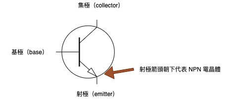
Its primary characteristic is that when a forward bias is applied between the base and the emitter, because of the base’s specific doping level, a portion of the moving electrons also flows into the collector (an N-type semiconductor), thereby establishing conduction between the emitter and collector.
In short, by controlling the input voltage across the base and emitter (high vs. low potential), we can control whether current flows between the emitter and collector, effectively creating a switch.
Besides acting as a switch, transistors can also serve as signal amplifiers; however, for the sake of brevity, we’ll focus only on their switching behavior here.
It is worth mentioning that when understanding circuits, the conventional “direction of current” we commonly talk about is actually opposite to the true flow of electrons. In a circuit, only electrons physically move. The reason we represent it this way is simply historical convention—people have long grown accustomed to the idea of positive-to-negative flow.
Logic Gates
Now, with a switching mechanism in hand, we can implement logic gates. For example, to build an AND gate circuit, we could do something like this:
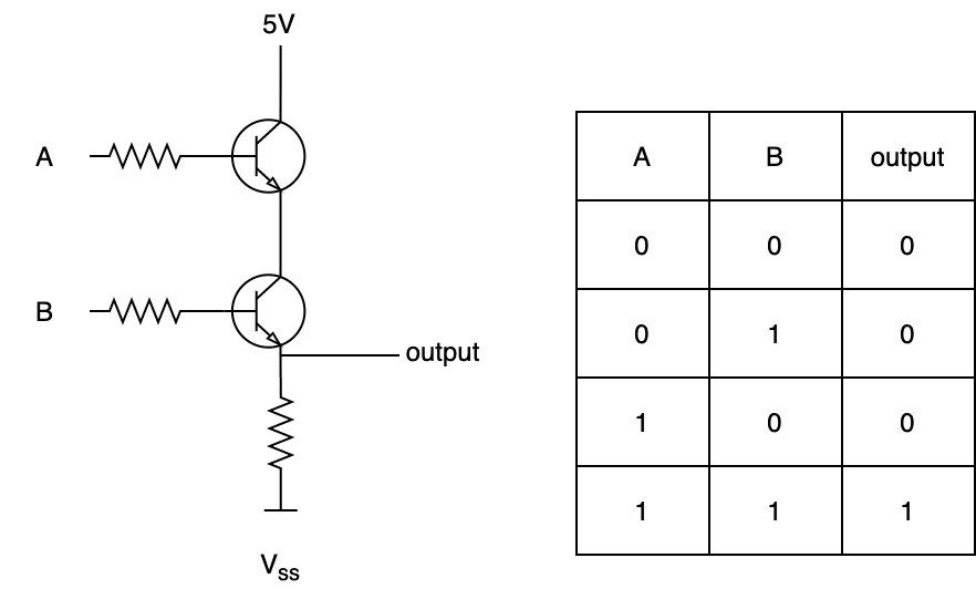
The entire circuit only conducts when a voltage is applied to both A and B, achieving an AND operation.
The image below shows the scale of a discrete transistor next to a keyboard:

The Semiconductor Industry
Although this kind of transistor is already quite small, it is obviously far too large for modern CPUs, where transistor counts reach into the billions. Consequently, the primary challenge of the modern semiconductor industry is figuring out how to pack more transistors into a limited surface area. In the 1970s, process nodes were around 10 µm; today, they have shrunk to 5 nm and beyond—roughly 2,000 times smaller than in the 1970s.
Final Thoughts
I personally hope that semiconductor manufacturing might one day become accessible to regular households, much like 3D printing has. There’s no need for nanometer processes—micrometer or even larger scale would be fine, so long as everyday makers can fabricate integrated circuits of their own.
Upgraded Homemade Silicon Chips
From the look of it, as long as you have the equipment, making one isn’t impossible. However, the gear shown in the video is still quite expensive, and most homes don’t have the space for it. I wonder if a revolutionary breakthrough will emerge in the future that fundamentally changes how people build integrated circuits.
Related Posts
- When a Measure Becomes a Target: From the Window Tax to Pull Request Counts I once wrote a script to tally how many PRs I contributed in a quarter, how many reviews I left, and how many tickets I closed, hoping to use numbers to prove my output to my manager. My manager simply remarked that performance isn't just about output. Years later, I finally understood—when a measure becomes a target, it ceases to be a good measure. From the British window tax and the Hanoi rat bounty to evaluating developers by PR counts today, the underlying mechanism is exactly the same.
- Using Cloudflare Images for Image Storage and Transformation Putting an image on a webpage is the simplest task in frontend development. But doing it properly—including resizing, generating multiple formats, and withstanding heavy traffic—is actually an entire end-to-end solution. Eventually, I offloaded everything to Cloudflare Images, keeping only a single original image.
- Stop Using AWS Access Keys Access Keys are an easily overlooked security risk in AWS. By pairing OIDC with IAM Roles, GitHub Actions can securely operate AWS resources without storing any secrets.
- Database Primary Keys: AUTO_INCREMENT, UUID, and UUIDv7 Backend developers often face the choice of primary keys: should you use auto-increment or UUID? What about collisions? How does UUIDv7 compare to created_at + index in performance? Here are the design decisions and benchmark results from testing 20 million rows.